I had nothing to do with the creation of KiCad... but I have become a serious "fan". This page tries to persuade you to investigate KiCad, a free Windows or Linux application for designing printed circuit board (PCB) artwork. Kicad can also produce Gerber files, the files for machine PCB production, or you can use my guide to making PCBs by hand. (If you use OSH Park for PCB manufacture, they take the .kicad_pcb file KiCad generates. You don't need to... but can if you wish... to create Gerbers.)
If you are new, and willing to work through a tutorial which will guide your first steps, give you the basic concepts and terminology, which I hope will empower you to go on quickly to become a KiCad wizard, then I would recommend......
KiCad is a free PCB design tool. Even if you do not settle on Kicad as the PCB tool for you, the tutorial will introduce you to some broad facts of PCB design life.
If KiCad doesn't seem to be what you want, I offer a page about alternative PCB CAD packages.
If you are already convinced and started, there are some good tutorials on using KiCad from CuriousInvestor. There's another good tutorial from David Jahshan.
I've done a separate page about adding libraries and modules (and trying to explain what they do). It takes as an example adding what you need to do design work for Arduino shields, but the original Arduino, and the Mega.
First I will say a bit about why I like KiCad
Then I try to give you a sense of a first session with KiCad.
And then there are some comments from another user.
I've been making PCBs (printed circuit boards) as a hobbyist since about 1980. As you might have guessed, my methods have changed over the years, but I have never invested a lot of money, nor, for that matter, done so very many boards. What I do is simple, but it meets my wants.
I used a big, expensive PCB CAD package for years. I've given Eagle a try. And now I'm on to KiCad.
I've used KiCad quite a bit, now. And for my wants, it has been very satisfactory.
If something doesn't work, being free is not enough.
But if something does work, being free is pretty marvelous. And, at least in the world of computers, it does seem as if there may be exceptions to the rule that if something seems too good to be true, it may not be true. There are excellent free applications available... e.g. the marvelous Open Office. Have you tried the database? And, if you are technically minded (okay... a geek... which seems likely if you're reading about making PCBs, you really ought to check out the Arduino microprocessor system.
All three share another important virtue: They are multi-platform. When my last shackles to the increasingly unattractive Windows fall off, and I move to Linux, I won't need to find a new PCB CAD tool. Or wordprocessor/ database/ spreadsheet. And I can still work with Arduinos, without scaling another learning curve wall. Hurrah for multi-platform. If only Textpad came in a Linux version!
Anyway... as I was saying... KiCad had, when I first created this page, earned hours of my time for being very promising. Since then, I have spent many happy hours in KiCad-land, and have not the least twinge of hope for anything else. Recently the people who make my PCBs, OSH Park, seemed to be "on the same page": They now accept KiCad files, saving me the hassle of exporting my designs to Gerber. (Which KiCad can do... but it is still nice that I don't have to do that any more.)
----
No powerful application is ever going to be easy to use straight away. You might be able to drive a tricycle without help, but if you had the chance to fly a fighter jet, a little work beforehand would be necessary wouldn't it?
KiCad "ticks all the boxes" as far as my PCB design wants are concerned.
It is nimble. The design procedures... once you get the hang of them... are easy to use, and "powerful". (I use the word sparingly.) It is flexible... I can design new symbols to go into schematics, and then link those to "foot prints" (my term for the outline and pads, etc, needed for the actual PCB design.)
So... that, I hope, is enough wittering by me. We now come to the second part of this page...
I've been writing guides for hobbyists for years... so I was delighted to find that someone else has done the work for KiCad!
This section is a bit dated. You can proceed with it, if you want help with the guide which helped me get started. Or, you can go to my "standalone" guide to using Kicad. (It is vastly superior to this, once you are ready to really study the details of using the software. What's here remains only to give you an easily accessible way to assess the hardware.)
That (my standalone) is very... "thorough"? You won't get far in a casual, skimming visit. If you'd like a less comprehensive guide, a "tour" rather than a "graduate course", maybe stay here. You can always go to my thorough guide later, if the tour convinces you!
---
I used the excellent introduction to KiCad by Teho Labs to get me through my first KiCad session. I'm pretty sure that was there in 2011, and it is still there in February 2017. I guess Teho like KiCad, too!
The Teho guide does an excellent job of showing the beginner the parts of a KiCad project. Sometimes one of the big difficulties with a new application is knowing where to start, what is possible, what is important. The Teho Labs guide shows you a project from start to finish. (As does mine, for that matter.) (Teho produce the Eridani, an inexpensive development board for the LM3S3651 ARM microcontroller, with a development environment to support it. They also produce the Cygni, an ARM header style development board for the LM3S3N26.)
However! Back to KiCad.
Well... "quick" relative to an introduction which should leave you ready to design a PCB yourself.
In case it wasn't clear: This introduction is heavily indebted to the Teho quide.
The steps... And yes, you do have to draw a schematic first. You can't, and, sorry, should want to, "just" do the PCB. This workflow is common in PCB design environments.
(I have deleted some "install" notes which were here, given the progress the world has made with making setups straightforward.)
Years ago, at the end of the install process I was told that to edit or create 3D object models, I would need Wings3D.
I have to say that Wings3D... Open source, Windows, Linux and Mac... was tempting. But I stuck to the "toy" I'd started with! A way to create a 3D visualization of my board is not in my list of wants, so I clicked "Finish", and moved on.
In June 2016, a new 3D viewer was released for KiCad. I don't know if KiCad still needs anything of the Wings3D suite.
As suggested in the tutorial I've recommended, after you start KiCad, you can just click "File | New". That lead to a SaveAs dialog. I don't like my data (project files, for instance) being outside my Windows "MyDocuments" folder, so I not only assigned a name, but first moved to MyDocs, created a KiCad folder, and a FirstProject folder in that.
A quick digression: If you have used computers mainly for nice "simple" things like basic email, etc, then you might need warning: With bigger applications, the concept of "a project" emerges. PCB CAD is one such application. For a single board, even one sided, you will have a project file (among other things, it keeps track of what else is in the computer relating to the board (or boards) the project is about!), a file with the schematic for the board, a file with the layout of the tracks on the board. Etc. Hence, the wisdom of files.
The "File | New" that we have done so far merely starts a new project. In a moment we will start the schematic for that project.
To proceed, you would...
When the design if finished, you send it to a commercial service to have your PCBs made.
I hope that gave you the idea?
When I tried to do a simple a board for an LED and a resistor when I was just starting with KiCad... I succeeded! IT was crude, and not without flaws, but the schematic and PCB would have "worked."
Here's the tour again, with more detail. The images are of the interface for an old version of KiCad, and details will be different, but I used that old version. Broadly speaking, the system behaves more or less as it did back when I did this part of the page. It was about 2010, I think.
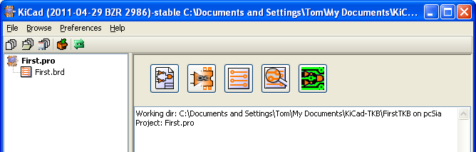
This is the main project manager window. It is the heart and brain of the design process.
In the left hand panel: Those names reflect the fact that I called my project "First". The names of the folders the project is in... showing at the lower right... make that less ambiguous in its wider context.
Above "Working dir", there are five icons, which you single-click to invoke different tools. (If you installed the software for 3D visualizations, I suspect there might be another.)
They are for, which you can see by hovering your mouse pointer over them...
Don't be too wedded to the Windows "Select, then issue command" methodology. In many parts of KiCad, if you have the pointer (or cross hairs) over something, it is already "selected", and pressing a key will execute a command. For instance, once you have a schematic started, put the cross hairs on, say, the LED, and press "r". The LED should rotate in the design.
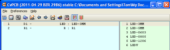
The following may help you with "CvPcb". It shows you roughly what you should have after assigning footprints..
The following may help you with "PcbNew", the PCB designer...
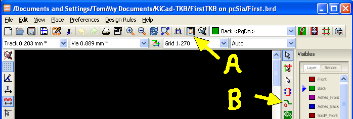
The "Read Netlist" button is marked "A" in yellow, above the "Grid 1.270". (The units were set to mm when the screenshot was taken.)
The "Add Tracks and Vias" button, is marked "B" in the above. Lines should appear to show you where tracks are needed. You create tracks to implement the rats' nest by clicking on one end of a track's path-to-be, and then drawing where the track should go, clicking to "pin" it down, to make a corner, double-clicking to end a given track.
However, I hope you haven done the "nutshell quick taste". If, like me, you went to theTeho KiCad tutorial, I hope that you also found that all went well... I was very impressed by the online component creator. (But don't use it. I prefer to be self-sufficient.)
At this stage, my page about KiCad becomes for a time a guide to the Teho guide! (IU hope the Teho guide is sufficiently un-revised to make this easy!)
Up to a certain point, no comment is needed. When I got to...
"Everything looks nice on our preview, click build library component. This will give us a file to save. Let's rename it on save as "myPartsC" and save it a new directory under our project's folder called libraries."
... which WORKED... but not quite as you might expect/ hope. I had to do a little "manual" work, moving the file with my component around on my hard drive. No biggie. (This process is somewhat different in 2017 from what it was. What is says here may give you an idea of what was done. But use my longer (and revised 2/17) guide to a similar exercise to actually try the software.
Going back to the online component builder....
It is a fault in my makeup that I always do things the hard way. Someday, I will master creating components with KiCad's native tools. However, as a newbie, it is very helpful to have the tool... and it will help me get started on the ultimate goal of being able to create components myself, without help, as I will become aware of the questions to be answered along the way of designing something.
So... as I said... the online component creation went well, but I had to do a little moving, renaming of the result. Calling it AAmyParts will put it at the top of library lists.
I didn't quite follow the tutorial instructions. I put the library in "MyDocs/KiCad/TKBLib" ("TKB" signifying me.)
Wow! Cool! When I got to the "move things around" part, I was a bit lost at first, but eventually I found that pressing m put me in move mode. I then had to drag out a box to include what I wanted to move, and as soon as the drag out was done, a subsequent drag moved what I'd selected. Hard to explain, a DELIGHT to use.. and I've used many applications which need a similar facility, but fail to make it as easy to do!
Let me digress to remind you: I hope I convinced you to have...
... all open on your screen. Read a bit of the Teho, see if there are comments here, try what you've been told to, and then proceed to the next thing to try.
End of digression!
The tutorial, when I (mis?) read it told me to put an NCP551, a diode, a capacitor, a 3 way general connector, and two grounds on the schematic. From the graphic below the "Now move the parts around till they look something like the screenshot below.." bit, it seems we also need a second capacitor... I added mine by right-clicking on the first, and using "copy", and a 2 way general connector, which I added with "a", "CONN_2" command.
Proceed with the tutorial I recommended... but be sure to save your project, shut down KiCad, and restart from time to time... just to be sure all is well... (^_^) I did not have problems... but you know the feeling of getting into something, and then losing a lot of work? And you're just getting started with KiCad...
Three little "things": As you stumble along, trying to get to grips with all of this...
a) Remember that ctrl-Z will often undo things.
b) Pressing the "escape" key will often get you out of things.
c) KiCad is "mode based"... you are usually in some mode... a "select" mode, or a "move it" mode, or a "draw wire" mode, etc. Getting to grips with this can be a little annoying... especially knowing what mode you are in, and how to change modes... but it is a common way of working with things like PCB design, and seems, to me, to be well implemented in KiCad... once you get the hang of it!!
Before you proceed with the tutorial, read this...
In a moment, in the tutorial, if it hasn't changed, you will read...
"You should notice two things on my schematic you may not have done a small X and two labels of VDD. If you attached wires delete them. (You can right click, use the del key or the eraser icon). See the X icon? That is the not connected, use it or place -> no contact flag to add the X to the N/C pin."
That appeared just below the wired up schematic I am about to talk about. For now, just DON'T try to make the small X (it is on pin 4 of the NCP551), don't try to add the VDD labels, don't try to make the wires to the VDD labels.
Using the "wire up" tool could be explained more thoroughly in the tutorial I recommend... or here... but it isn't. I'll mention two things: Use the escape key to abort a misplaced wire. To join two points (once you are in the wire-up mode), just click on the first, then click on the second. Click at intermediate points to create nodes in the wire.
Right! I hope you have your schematic almost like the one on the tutorial page?
First "the X"
You need to create a "no contact" flag on pin 4 of the NCP551. It is a small "x". You add it by using the menu "Place|No Contact Flag" route, or by using the "q" shortcut.
Now the labels... there is text about them in the tutorial. I think the thing is that you have to put the label on the schematic FIRST, and THEN connect wires to it, and those wires to existing wires in the schematic. That's what I did, anyway!
The tutorial then comes to "You could run a DRC check now and eeSchema will try to help you find where you made mistakes...". At 8/11, I think "DRC" had changed to "ERC", under the tools menu. I didn't get errors, but whether you get errors will probably depend on how you got to the result we should all be at by now.
I used "Tools|Generate Netlist" to do that.
Next the tutorial says... "We are done with eeSchema, you can close it." When you close eeSchema, you should find the main KiCad project manager still running, underneath the eeSchema window you just closed. Proceed as directed in the tutorial.
Don't, by the way, double click on the icons for eeSchema, single click. (If you double click, say "no" to "... already running...", and look underneath the main project manager for the sub-module you tried to start twice.)
While assigning footprints, I couldn't find the promised C1V8, so just used the suggested alternative CP4.
At this point I found a typo in the value assigned to one of the capacitors. I just closed CVpcb, reopen eeSchema, changed the value, regenerated the netlist and proceeded with the tutorial.
I got a bit tangled, trying to make my pads just how they were meant to be. I think that part of the problem may have been that the tutorial may have been done on a system configured to work in inches whereas mine, at the time, was running in mm. But I just pressed on, with not-quite-right pads. No big deal. I was still liking KiCad!
When I got to "Add a line around your part..." I could have done with more help... but managed eventually. Select "add graphic line" from the mini buttons on the right side of the window. Click to start line. Click again to end a segment. Double click to finish the outline. I didn't find a way to drag a corner, but I just deleted bad segments, re-drew them.
So now you've got to "...Now we, will save it to a new library..." Do that.
I'm very new to KiCad, but my gut feeling tells me something I really like...
I think I can use KiCad supplied libraries... supplemented (when necessary) by "general" libraries of my own creation... supplemented (when necessary) but project specific libraries.
Furthermore, if my guess is right, all of these libraries are going to delightfully "easy" to manage, keep straight, etc. I say "easy" because such a subtle task will never be "easy"... but it seems KiCad is well designed, and the task may be as "easy" to accomplish as possible.
Also, the libraries seem to be contained in text files... opening the way for user study, tweaking, etc.
KiCad seems to keep the specifications for what appears in a schematic and what appears on a PCB design separate. In some cases there will be a 1:1 mapping of the schematic and the PCB elements... but it also seems that you can "overlay" several schematic elements on one PCB element. For instance, while the schematics for a simple resistor and a simple diode will be different, if you don't mind not indicating the polarity used for the diode, the same PCB element could be used for both. This seems good to me. Efficient. Elegant. Labor saving.
I got to... "Go back to the module editor and 'select working library'" in the tutorial, got stuck. I'd missed the "Go back to the module editor". Once I'd done that, I looked for "Select working library" in the menus. Didn't find it. But DID find it as the first icon on the toolbar across the top of the window.
Did what the tutorial told me to.
"Click on the LDO GND pin" means click on pin 2 (middle pin of the three on one side) of U1, the NCP551 Low Dropout voltage regulator component. (I don't know what the "O" comes from... perhaps a French equivalent of "Regulator"?) If you zoom way in on U1, you can see the pin name and number. (Cool in itself! (The zooming))
The tutorial speaks of... "There is one thing we don't like which the autorouter did and that was to place the trace to the diode on the backside, so I am going to delete those traces and route them myself, using the delete key and the routing tool. Try to do this yourself."
These are tremendously important skills. Play around a bit with modifying tracks. While you are doing that, don't be distracted by the fact that a rat's nest line can look a bit like a segment.
Here's what I mean: At the start of laying down the tracks, you had the rat's nest lines. They showed you the connections which would have to be made, if your PCB was going to realize the schematic you designed. Your job, and you used the autorouter to do much of it, is to decide where to create tracks in order to achieve the connections dictated by the rat's nest. As you do that work, it is possible to mistake a rat's nest line for a track (trace), or vice versa.
"Finally choose update module in current board."... you do this with a toolbar button at top of screen- the eighth from left on my toolbar.
That little exercise was interesting... but raises a little concern: Where is the module defined? I suspect that a "base" definition exists in the libraries, and that the project has some "library" of tweaks to designs, tweaks which apply to the module just in that design. Could be a path to chaos... but also a useful opportunity, if kept under control...
Whew! Pretty cool. The tutorial tells you about exporting files for PCB fabrication services... using the requirements of "BatchPCB.com" as an example.
If you want to produce your own PCBs by hand, by the techniques explained in my page about how hobbyists can make printed circuit boards, PCBs, then you'll want to know how to selectively print elements of the board. Here we go...
It is only a matter of using "File | Print". To print the tracks of the top side of the board we just developed, select...
Copper layer: Front
Technical layers: PCB_Edges
... and use your common sense on some other choices
(You are an exception to the bumper sticker truth, "Common Sense Isn't"... aren't you?)
Perhaps not for this, but sometimes you will want to select "Mirror"
Use the very good "Print Preview" to see what you will get, before wasting paper and toner.
Not "necessary", but perhaps of interest:
Ever since you started working on the project, around the area you've been working in there's been a red rectangle, made up of twin thin lines. And in the lower right, there's been an engineer's "info box" with the project's file and sheet number, a title, etc, etc.
You can change the size of the box, and tweak the contents of the info box via the "File | Page Settings" menu option, present in the PCBnew page.
Sigh. That makes the third PCB CAD package I've spent hours getting to know a bit about. And I like it, at 8/11. Looks like the hours I spent trying to learn the other two were partly wasted.
It is early days yet... maybe I will find something in KiCad that I can't live with... but I suspect I won't.
I'd like to tell you that I do lots of PCB design, and that if I still like this later it means the package is great. Sadly, I don't do enough design work... yet!... to be a knowledgeable critic... but maybe with this good tool I will start doing more PCB design work!
Whatever. I hope that the above at least gave you an idea of some elements of KiCad, and maybe helped you go through the excellent Teho Labs tutorial even more easily than I went through it.
I saw a useful contribution by Raron in a discussion of PCB design software for hobbyists at an Arduino forum, and decided just to pass on large bits. I have his permission! They have been edited. (You might want to visit Raron's blog... some fun stuff there!)
Raron liked the fact that if you have EEschema and PCBnew open at the same time, and click on a pin, the corresponding pin and track is highlighted in the other program. The pointer isn't boldly highlighted EEschema. He finds the track highlighting handy.
In addition to the built-in tools for track routing, KiCad can also export the net to the online router at http://www.freerouting.net/. He wrote that he usually routes things himself but that either KiCad's own routing routines or FreeRouting's (the latter, I think) has a nifty "track pushing" feature which repels other tracks.
Raron, too, found the interface less than intuitive, at first, also citing..."KiCad can be somewhat quirky to work with, I guess mostly because it is "mode based"... you are in "move objects" mode, or "connect wire" mode, etc. Also, the KiCad approach to making custom library components/symbols and footprints ("modules")..." isn't just YACP.... yet another CAD package. I (TKB) for one am delighted! I will happily scratch my head a bit when I start with an application if they have found a new way to do things. To get to someplace better, you have to go places you've never been, as they say.
Raron (and I) like the fact that you can mix and match components with custom footprints on a per-project base. (But you can also make custom footprints available globally.)
If you want to use the 3D visualization tool in KiCad, you may want to visit http://www.kicadlib.org/Fichiers/Ludek_libraries.html. When I took Raron's advice and visited the page, I found it well organized and modular. I downloaded the .zip files for two components, and they had .wings files, which I presume KiCad can access directly. They didn't seem to have the KiCad files for schematic design or PCB layout, though. They did (sometimes) have small .gifs with information about the part, e.g. the sort of illustration you see on a supplier's web page, and (in the .gif) text with things like the component's ratings. KiCad provides a tool for linking documentation to components, which seems like an excellent idea to me... Now... will I get myself organized, and use the tool?. I'm not sure if .gif files can be linked to components in KiCad, but it seems that .pdf files can be, and you can make the latter from the former.
And now for a little digression: While working on this, I was trying things on KiCad, to be sure I was being accurate. SOMEHOW, I'm pretty sure it was clicking a "View documentation" or somesuch, I brought up a .pdf file called "footprints". I can't figure out how I did it, and I can't find the file on my machine!!! But it is worth looking for. It is a useful reference document showing you lots of things, saving you hunting with the component viewer. If you re-discover how to bring it up, please tell me!! (I did FIND it again, anyway... It was in...
C:\Program Files\KiCad\share\modules\footprints_doc)
Also as I was working on this essay, for the first time (blush) I gave KiCad's "help" a try. Well worth a visit. Not only does it have the usual, but it also has lots of notes on recommended working practices....
Anyway... back to what Raron contributed to the discussion...
Raron himself offers some KiCad libraries at a page on his blog. The title says "RGB LED stuff mostly", but we all know how the contents of a folder sometimes grow after a name is chosen!
I have made a start on a guide to installing third party libraries and modules for KiCad.
But I've saved Raron's main contribution to last, because, while it is a major contribution, it won't be important to a large number of readers. But everyone should be impressed that what he is going to talk about is possible.
Raron says (edited)... "Personally I use more than one computer, and more than one OS. I favor Ubuntu for working on my stuff. One thing that annoyed me a bit was the need to manually re-add the libraries used in any given project, if you suddenly find yourself at another computer for a while. Yes, there is a "user defined search path" list or setting, but I haven't had much luck with that (newer versions of KiCad might have fixed this?). Anyway I found a solution that worked for me using symbolic links. That approach may restrict it to one user per PC. Working across network drives might be tricky, too." But! If you want to know more about Raron's answer, you can read about it at the link I'm about to give. Note that this idea has ramifications for many similar wants. It doesn't just solve KiCad hassles. Click here for Raron's hassle-free project sharing using symbolic links. (I think a "symbolic link" is how things like the Windows "My Documents" folder are created.)
![]() Page tested for compliance with INDUSTRY (not MS-only) standards, using the free, publicly accessible validator at validator.w3.org
Page tested for compliance with INDUSTRY (not MS-only) standards, using the free, publicly accessible validator at validator.w3.org